
Citation: Denna E, “Using Simulation and Modelling Versus Prototyping for Medical Radio Frequency Design”. ONdrugDelivery, Issue 124 (Sep 2021), pp 67–71.
Enrico Denna looks at the advantages of a simulation and modelling approach over prototyping for the design of medical products.
“Several medical devices are becoming even smarter and more connected, storing big data, using apps and enabling functionality
that substantially benefits users.”
The growth of technology and end-user expectations are ever more important factors in many application areas, and medical devices are at the forefront of this innovation process. The requirements of an increasingly connected world have had a significant impact on electronic design and specifically on the area of radio frequency (RF), which, by its very nature, represents a major design challenge. Modelling and simulation are valid instruments to assist in meeting this challenge because electromagnetic design performance cannot be easily predicted in advance by relying solely on the designer’s experience.
The world is becoming increasingly “smart”. Less than 10 years ago, the smartphone was unknown, while, today, smart devices, connectivity, apps and data connection are ubiquitous parts of our vocabulary and our lives. Medical devices have naturally followed this trend and have adopted connectivity as a must-have feature to align with market demand. Several medical devices are becoming even smarter and more connected, storing big data, using apps and enabling functionality that substantially benefits users.
The design of these new features presents several challenges – one of the most critical aspects being the creation of a stable and reliable connection within a user-centric usage model. Here, we are talking about wearable models where devices are powered by smaller, sometimes non-rechargeable or non-replaceable batteries; devices that are typically either handled by, or are directly in touch with, the human body, such as insulin pens or drug delivery patch plasters; and devices that are used or stored in varying environmental conditions, not only at room temperature at home but also in the mountains, inside a car or kept in a refrigerator. These new design requirements have spurred the creation of simulation tools to help designers refine their projects while saving time and costs during development, which, until now, has always been undertaken using trial-and-error. HFSS by ANSYS 3D electromagnetic simulation software is one of the most powerful tools available to assist designers with their projects.
THE BENEFITS AND ADVANTAGES OF SIMULATION
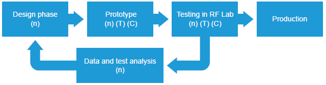
Figure 1: Standard trial-and-error approach. Final cost of the process is calculated according to the (T)ime and (C)ost of prototyping multiplied by the number of prototyping iterations (n).
A comparison of process flows reveals that, in a trial-and-error approach (Figure 1), the number of design phase iterations (n) to fine-tune and adjust the design results in an equivalent number of prototypes and tests, which must be conducted in an external lab with the RF instrumentation and accreditation to issue a formal certification. The cost of this process (C) is calculated from the costs of the prototyping and external laboratory testing, while the time to mass production (T) is derived from the time it takes to construct the prototypes, book the external labs, conduct the tests and issue the test reports. All these steps must be multiplied by n.
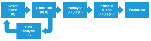
Figure 2: Simulation approach. Final cost of the process is calculated according to the (t)ime of simulation multiplied by the number of simulation iterations (n). It is evident that the cost of the trial-and-error approach (n*T*C) will invariably be higher than that of the simulation approach (n*t + 1*T*C).
In the simulation approach (Figure 2), n only affects the number of simulations that may take a time (t) of some hours or days depending on the complexity – this time is obviously significantly shorter than the weeks necessary to realise and test a prototype. Furthermore, the only person involved in a simulation is the designer, while any prototyping test involves several experts (layout engineer, purchasing office, test operator, local prototype producer and financial office).
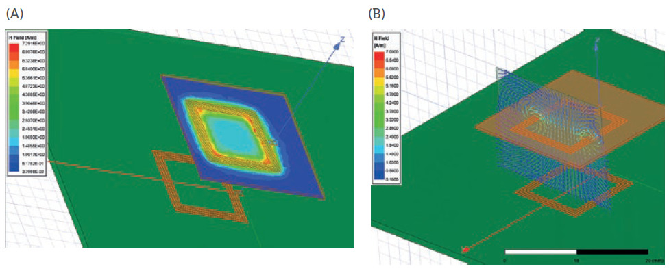
Figure 3: Modelling and simulation of an RFID tag with its reader.
“Simulation plays another fundamental role here by providing a model of the human body complete with skin, bones and internal organs into which it is possible to introduce the device to study its behaviour and the effect on the radiation patterns.”
Another disadvantage of prototyping is linked to the time needed to take delivery of the prototype, during which the designer is unable to work on this project. Taking all this into consideration, it is clear that the prototyping process is inefficient and easily justifies the investment in a simulation tool, which can be amortised in just a few years of design activity.
The improvement realised by the introduction of simulation is clearly evident in some design examples. Figure 3 shows the modelling of the coupling of an RF identification (RFID) tag and reader the simulator enables the engineer to replicate the coils of both the tag and the reader (Figure 3A) and then to examine the magnetic field coupling between the two elements according to the spatial distance (Figure 3B).
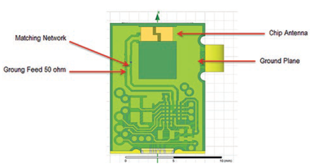
Figure 4: Example of PCBA with a chip antenna.
Electrical designers typically begin by focusing on the printed circuit board assembly (PCBA) and Bluetooth antenna design, applying their experience and RF knowledge to implement the application notes and guidelines of the RF module and the integrated or chip antenna selected. This leads to a PCBA design that respects the ground planes and transmission lines and has controlled impedances, which then guides the layout engineer to design the microwave traces with the appropriate thickness and dimensions (Figure 4).
However, this approach may be inadequate – the mechanical parts of the device, particularly where there are multiple boards assembled together, and the metallic parts, such as the battery body, motor engine or display holder, can significantly affect the electromagnetic field. These side effects are difficult to predict in the trial-and-error approach, resulting in an increase in n. The simulator makes it possible to import complete mechanical and electrical files (such as STEP and BRD files, for instance) to obtain a complete model of the device in which it is possible to assign a material to any component using the simulator’s internal library.
Figure 5 shows part of a pen-shaped device into which the PCBA illustrated in Figure 4 has been introduced and connected to a micro-USB connector. The device housing is made of steel with a rechargeable battery on the back of the electronic location. The PCBA is connected to the housing via a pogo pin that grants a ground connection.
This set-up and similar systems can dramatically affect both the RF transmission and the Bluetooth antenna. Once assembled, as shown in Figure 5, this system has a completely different radiation pattern compared with the initial configuration visible in Figure 4.
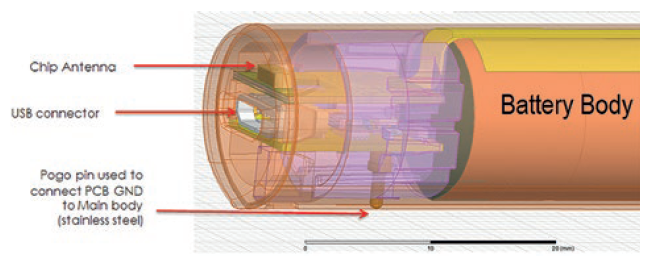
Figure 5: A 3D design of the final device including electronic PCBA and
mechanical parts.
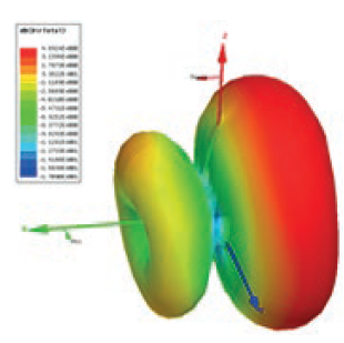
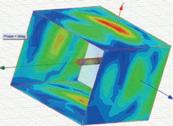
Figure 6: 3D radiation lobe.
Figure 6 illustrates the 3D radiation pattern generated by the simulator, which immediately informs the designer that the best direction for radiation is on the back, as opposed to on the body of the battery. This could be due to internal reflection caused by metallic parts or to the mechanical portions of the opening, both of which are compatible with this wavelength.
This result is very unusual, and therefore difficult to predict. The simulation result has therefore avoided a prototype round because, previously, the only way to have discovered this behaviour would have been to test a prototype and then to rework the device to increase the performance in the forward direction; the simulation allows this behaviour to be addressed in advance.
The simulator makes several pieces of data available both graphically and numerically: 3D radiation lobes, animations of 3D phase radiation (Figure 7) and impedance and Smith charts suitable for S11 tuning and power transmission (Figure 8).
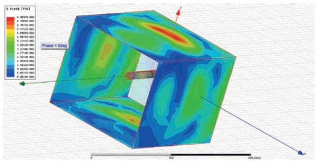
Figure 7: Animation of 3D phase radiation.
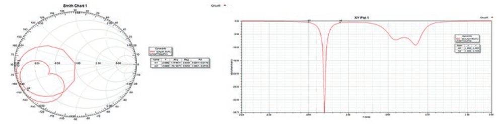
Figure 8: The simulator provides substantial engineering data. Here, you can see the Smith Chart and the S11 parameter suitable for antenna tuning and Q factor definition.
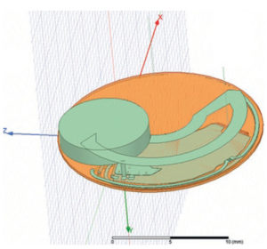
Figure 9: Metallic antenna derived from the battery clip.
“The clear advantages of the simulation approach are motivating more companies to consider investing in these tools to improve their design processes.”
Simulation makes another major contribution during the design of a PCB antenna. In the trial-and-error approach, the application note or reference design are often only indicative (and sometimes ideal). This generally increases the number of iterations required because it is not always possible to rework the antenna, particularly for high radio frequencies where some tenths of a millimetre in the track dimensions can make a difference. An innovative solution could be accomplished using an antenna derived from the metallic parts already present in the mechanical device (Figure 9). Such a design would be easier to simulate several times before moving on to creating a prototype device once the engineer is closer to achieving the final solution.
In medical and wearable devices, the effect of the human body is not negligible –microwaves generated by Bluetooth or Wi-Fi connections are absorbed by human tissue. Simulation plays another fundamental role here by providing a model of the human body complete with skin, bones and internal organs into which it is possible to introduce the device to study its behaviour and the effect on the radiation patterns.
Figure 10 shows the simulation of a Bluetooth device attached to the shoulder of a patient. The field strength is measured at the level of the trouser pocket, which is where a smartphone would usually reside while receiving the data. This simulation allows the designer to better understand the result and the reference direction of the radiation in the presence of a human body, making it possible to tune the design and also gain useful information for the usage model. It also provides an indication of other safety parameters, such as the specific absorption rate.
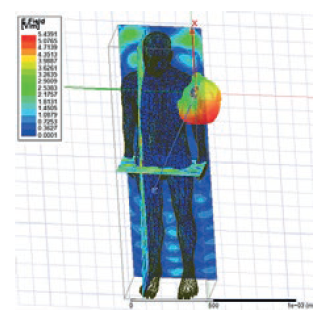
Figure 10: Human body model available in the simulation tool.
To optimise the confidence of the simulation result, the model can be validated during the first prototyping round. In this case, the results of tests carried out in an anechoic chamber using RF instrumentation and possible human dummy material (Figures 11 and 12) can be compared with the results obtained with the simulation, allowing the simulation model to be fine-tuned by adjusting some of the parameters or corrective coefficients in its configuration. After this final step, the designer has a powerful model that truly represents the functioning of the device inside its usage environment and that can be easily used to evaluate modifications, or as a reference for similar new devices.
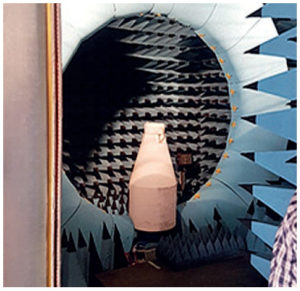
Figure 11: Measurement of a device in an anechoic chamber
using a biological dummy.
The power of this tool can be supported by other subtools, such as Optimetrics, which enables a parameter to be optimised or the optimal coefficient of the design to be found using automatic and iterative simulations. Other tools and add-ins can also be introduced to support thermal or impedance simulations.
The clear advantages of the simulation approach are motivating more companies to consider investing in these tools to improve their design processes. There are several benefits: the cost and time savings during production, the improvement of the designers’ know-how and competence because of the ability to experiment (and thereby increase their knowledge and motivation in a field that is not always intuitive or easy to master) and, last but not least, simulation provides a structure to the design process that will inevitably be recognised by customers who will appreciate a more professional approach.
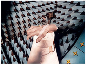
Figure 12: 3D radiation pattern measurement in anechoic chamber.
Based in part on an article that first appeared in Enginsoft’s Summer 2021 newsletter, No 2.