
Citation: Kim Y, DeMello D, Wilson P, “Specialty LCP Compounds for Electronics Integration in Connected Medical Devices”. ONdrugDelivery, Issue 121 (Jun 2021), pp 37–42.
Young Kim, Don DeMello and Philip Wilson, discuss the benefits of recent advances in liquid crystal polymer for connected medical devices.
“Vectra MT LCP polymers are a natural fit for pushing the envelope on thin-wall designs to free up more internal space without sacrificing product strength, stiffness or dimensional control.”
Remote monitoring of patient health, closed-loop control of therapeutic devices and the use of artificial intelligence for improving diagnoses through the analysis of continuously captured biometrics are all revolutionary ideas that show promise for improving patient outcomes and reducing the overall cost of healthcare. Full implementation of each of these industry initiatives requires the connection of medical devices to other nearby devices and to the Internet of Things (IoT).
Empowerment of patients to monitor their own health indicators and make decisions through familiar user interfaces, such as smartwatches or mobile phone apps, is leading to a convergence of medical devices with common consumer electronics. As consumer electronics have evolved in the 21st century to become faster, more powerful, more compact and more affordable, speciality materials have met the challenges of that industry.
While Celanese has more than two decades of clinical history for the use of Vectra® MT liquid crystal polymer (LCP) in medical devices, Zenite® LCP compounds have been developed to serve the electronics market. In this article, the authors envision the benefits of recent advances in LCP compounds optimised for dimensionally stable precision microstructures, for dielectric properties enabling wireless communications and for patterning of circuits on structural device components for part integration and total device miniaturisation.
In the December 2020 issue of ONdrugDelivery, Michael Kiely et al highlighted design considerations for high volume manufacturing and tolerances in the electromechanical interface as critical components of a design strategy for connected devices.1 The authors further note the need for cross-functional expertise for optimising device reliability. In this article, the authors highlight the role that Vectra and Zenite LCP compounds are able to play in this industry-wide effort.
DESIGN BENEFITS FROM THE USE OF LCP
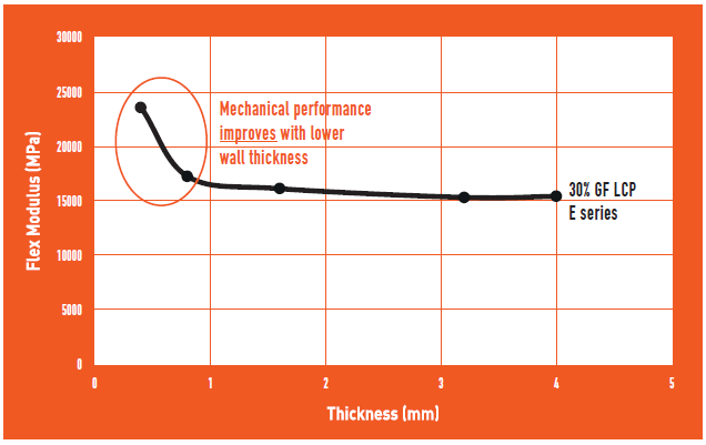
Figure 1: Paradigm shift in polymer thinking – design thinness determines LCP stiffness properties.
Medical product designers are seeking to increase the number of electronic and electromechanical components in tighter and lighter spaces for patient utility, comfort and concealment. Vectra MT LCP compounds have proven valuable for wearable, portable injector designs, diagnostic devices, injector pen internals, surgical staple cartridges, surgical instruments and microneedle arrays.
Liquid crystalline polymers are a natural fit for pushing the envelope on thin-wall designs to free up more internal space without sacrificing product strength, stiffness or dimensional control. LCP resins increase in strength and stiffness with thin-wall designs due to their unique rod like molecular orientation, with optimum mechanical properties below 1 mm, as shown in Figure 1.
For specific application needs, Vectra and Zenite LCP resins can be tailored through comonomer chemistries and additive compounding to produce optimal mechanical, dimensional, thermal and tribological properties. Due to the extreme shear-thinning behaviour of LCP, complex thin-wall designs that can’t be filled with other resins can be filled with LCP and a high microreplication of mould surface achieved – one reason why LCP is useful for micro moulded parts and microneedle arrays.
“For specific application needs, Vectra and Zenite LCP resins can be tailored through comonomer chemistries and additive compounding to produce optimal mechanical, dimensional, thermal and tribological properties.”
POLYMER AND PROCESSING CHARACTERISTICS OF LIQUID CRYSTAL POLYMERS
LCP compounds are unique in the world of engineering resins. LCP is a high-heat thermoplastic but its value for most medical devices is its exceptional flow in thin-wall designs. The morphology of LCP resin’s nematic rod-like crystalline structure is very different from amorphous and semi-crystalline resins. Even unfilled LCP is extremely strong and stiff, behaving like a self-reinforcing polymer, with similar or greater mechanical properties than 20–30% glass fibre (GF) composites.
As described in a Celanese white paper on high-volume manufacture of thin-wall medical device components with Vectra MT LCP,2 the material’s high flow combined with high stiffness and strength allows designers to make thinner structures without sacrificing structural performance, enabling smaller parts and liberating more internal space for pharma or other components.
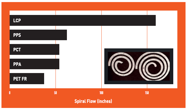
Figure 2: LCP offers superior flow and fill for thin wall structure and micromoulding details.
As shown in Figure 2, spiral flow characterisation of 30% GF LCP versus other 30–40% GF resins at 3.2 mm (0.125 inches) demonstrates the remarkable ability for LCP to fill long, thin channels compared with other engineering resins.
As illustrated in Figure 3, LCP has a low heat of fusion from its ordered molecular structure, which changes very little between its molten and solid phase – allowing a rapid cycle from melt injection to part ejection.
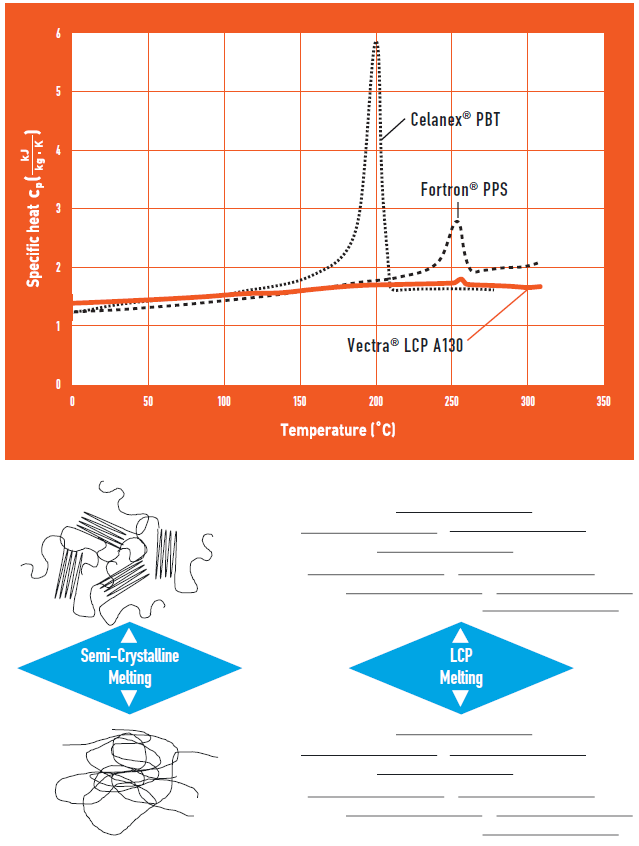
Figure 3: The unique morphology of LCP leads to rapid solidification and short moulding cycles.
“A higher Dk substrate allows the design of smaller antennas at the target signal frequency.”
Rapid cycling means higher moulding productivity, which leads to lower capital cost as fewer moulds are needed for high-volume production without the high mould temperatures commonly necessary with polyphenylene sulfide (PPS) or polyetheretherketone (PEEK). LCP can be processed at mould temperatures less than 100 °C, similar to many engineering resins and requiring only lower-cost, water-based temperature control units.
Other characteristics of LCP include:
- Excellent dimensional stability with low moisture absorption (0.03%) and low mould shrinkage (0.1–0.4%)
- Inherently flame retardant (FR) without FR additives
- Very clean, low extractables and ionics, food contact compliant
- Can be biocompatible with MT grades being US FDA master file listed
- Service temperature from -190 °C up to 240 °C, short term up to 340 °C
- High tensile strength (up to 185 MPa) and high tensile modulus (up to 30,000 MPa)
- Excellent barrier property to oxygen and moisture
- Sterilisable by steam, ethylene oxide, gamma radiation or H2O2 plasma
- Excellent chemical resistance
- Natural colour is opaque, off-white ivory with options for colouration.
TRANSLATING CONSUMER ELECTRONICS TECHNOLOGY TO MEDICAL DEVICES
In addition to medical devices, the benefits of LCP outlined above, combined with its thermal stability at temperatures used in common soldering processes and consistent humidity-stable dielectric properties at high frequencies, have enabled the reliable manufacture of high-speed electronic connectors of ever-decreasing size for electronic devices – beginning with personal computers and evolving into mobile phones and other connected consumer electronic and telecommunication devices from Bluetooth to 5G. As a broadly accepted, indispensable material for consumer electronics, Zenite LCP is a natural choice for the development of speciality compounds to meet adjacent needs for antenna substrates, micro-optical assemblies and circuits integrated into the framework or housing of these devices.
Antenna Substrates
Medical devices may potentially be connected using any of several communications standards, depending on the desired connection, be it to a patient’s personal device via Bluetooth or home WiFi network, to a 5G network for external monitoring via the IoT or to the Wireless Medical Telemetry Service (WMTS) for hospital use. Each of these require engineered antennas fabricated on low-dielectric loss substrates and can benefit from the ability to optimise the dielectric constant to the circuit or antenna array design.
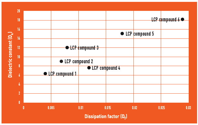
Figure 4: Dk/Df values for high Dk Zenite LCPs, measured via International Electrotechnical Commission (IEC) 61189-2-721 method at 2 GHz.
For patch antenna arrays, each microstrip array element will be resonant with the operating frequency, f, at a patch length, L, equal to approximately one-half wavelength in the antenna substrate which is dependent on the dielectric constant Dk… 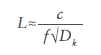
…where c is the speed of light. A higher Dk substrate allows the design of smaller antennas at the target signal frequency. In other design cases, low Dk improves signal integrity by reducing coupling between neighbouring antenna array elements. LCPs have a Dk for typical filled compounds of >3.5, depending on polymer composition and filler type. The dielectric loss, Df, can be less than 0.005. As shown in Figure 4, Dk can be increased through additives up to >20 while retaining the inherently excellent mouldability of LCP. The Df increases with increasing Dk but still remains very low. As most fillers will have a higher Dk than polymers, lowering the Dk is more difficult than increasing it. Yet novel compound formulations have been identified, as shown in Figure 5, that can reduce the Dk to 3.0.
Figure 5: Dk/Df values for low Dk Zenite LCPs, measured via IEC 61189-2-721 method at 2 GHz.
Patterned Circuits
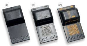
Figure 6: Example of laser direct structuring of circuit interconnects.
Antennas that are conformally integrated into devices may use flexible films or moulded articles as substrates. These substrates must be suitable for the robust processes required to pattern conductive traces on them to form the elements of the antenna or antenna array. Typical methods for patterning circuits on LCP may be screen printing or ink-jet printing of conductive inks followed by electroplating.3
Laser direct structuring (LDS) is an alternative to the printing of conductive inks. LDS uses a photoactivated additive to create conductive traces in the host LCP polymer which can then be selectively patterned through electroless plating to complete the circuit fabrication process. Figure 6 shows an example of a test part demonstrating the steps of this process, starting with a moulded part (A), then a laser-marked photoactivated surface (B) and electroplated interconnects (C).
Micro-optical Assemblies
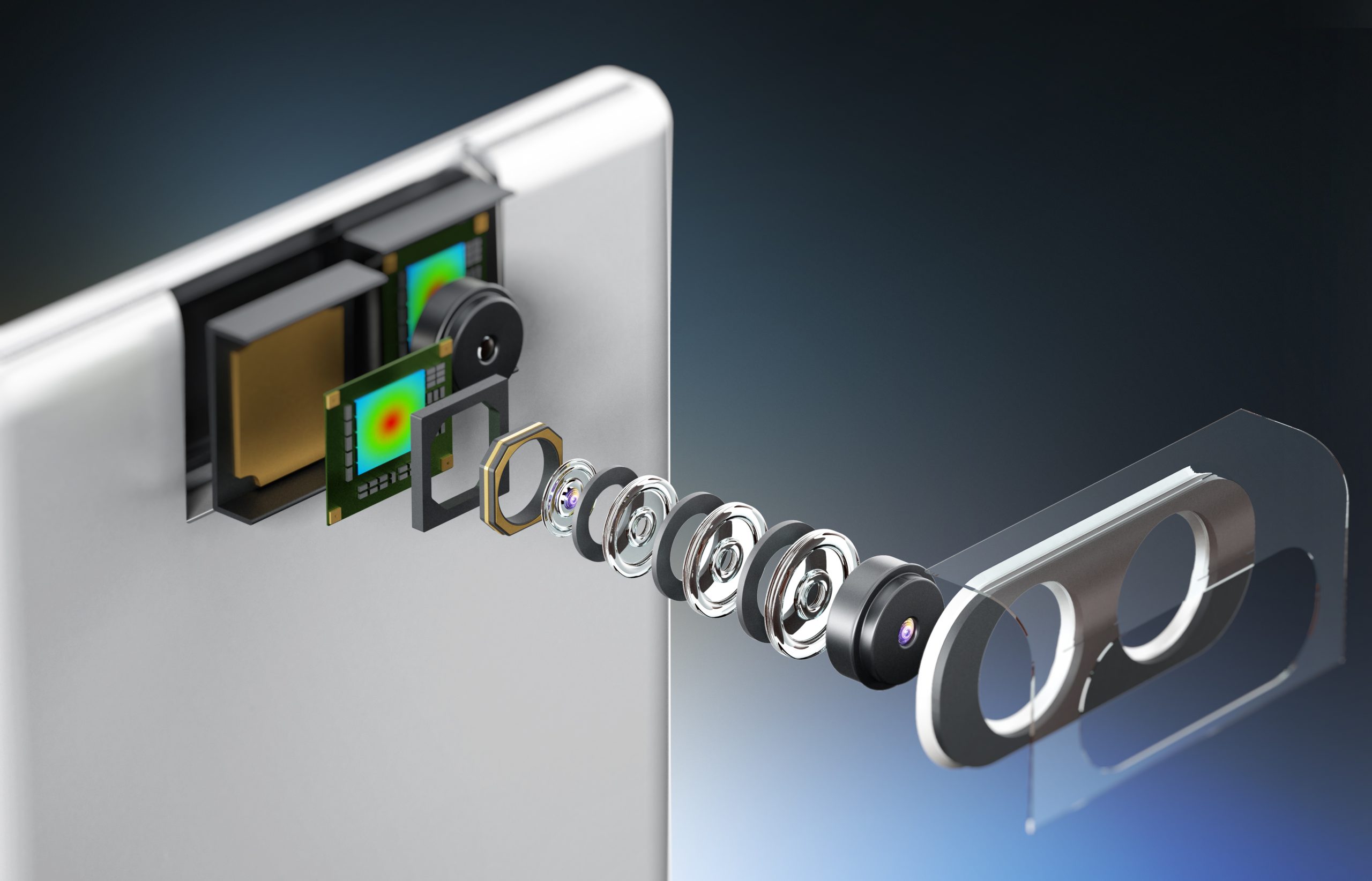
For the ubiquitous mobile phone, the incorporation of cameras requires precision manufacture of highly durable micro-optical assemblies to properly align lenses to the imaging array (Figure 7). These assemblies must be dimensionally precise and stable, durable against torturous use by consumers and capable of reliable production of hundreds of millions of assemblies per year. Zenite® LCP SEA30N is the leading material for the manufacture of compact camera modules for mobile phones.
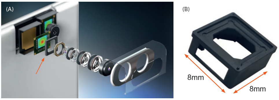
Figure 7: (A) Exploded view of compact camera (module frame identified by arrow). (B) Photograph of a compact camera module frame. Image courtesy adventtr / iStock / Getty Images Plus.
Many current smartwatches and fitness trackers and emerging wearable medical devices also rely on integrated optical systems for the photoplethysmographic (PPG) detection of volumetric variations of blood circulation.4 Continuous monitoring of heart-rate variability can be used to detect a plethora of cardiovascular disorders. Sophisticated machine learning algorithms can provide further insights into major medical risks for atrial fibrillation, stroke and cardiomyopathy.5
This powerful technology can be integrated into the wrist, torso, forehead or earlobe – with the potential to combine this function with other existing wearable medical devices, such as hearing aids and glucose monitors, or consumer products, such as earphones and smartwatches. This combination of functions into a single device is likely to benefit from further reduction of the size of the optical assemblies and, subsequently, from the translation of the well established technologies for the manufacture of mobile phone cameras – including the use of specialty LCP compounds.
SUMMARY
Connected medical devices promise to improve the effectiveness and reduce the cost of healthcare. Fortunately, the adjacent industry in consumer electronics can inform these solutions. Suppliers with a presence in both industries can provide unique insights and support to device designers in their product development endeavours. The Vectra and Zenite LCP lines of engineered compounds offer a translatable solution set, yet products alone are not a complete solution. The necessary innovations in how devices are designed, manufactured, regulated and secured6 call for a creative and collaborative problem-solving approach that relies on a new type of expansive thinking, less constrained by the solutions of the past and more open to creating the solutions of the future.
NOTE: Vectra MT LCP is the medical grade of Vectra/Zenite LCP developed and manufactured with the medical and pharmaceutical regulatory landscape in consideration.
REFERENCES
- Kiely M et al, “Medical Device Design Strategy for a Connected Future”. ONdrugDelivery, Issue 115 (Dec 2020), pp 14–18.
- “High Volume Manufacture Of Thin-Wall Medical Device Components With Vectra® Mt® LCP”. White Paper, Celanese, 2020.
- Jilani S et al, “Millimeter-Wave Liquid Crystal Polymer Based Conformal Antenna Array for 5G Applications”. IEEE Antennas And Wireless Propagation Letters, Jan 2019, Vol 18 (1), pp 84–88.
- Castaneda D et al, “A review on wearable photoplethysmography sensors and their potential future applications in health care”. Int J Biosens Bioelectron, 2018, Vol 4(4), pp 195–202.
- Kraudel R, Valencell Presentation, Medical Wearables 2020.
- Oakley T, “Top Five Drug Delivery Trends for 2021”. ONdrugDelivery, Issue 117 (Mar 2021), pp 8–10.